


COMPANY
Welcome. Hello.
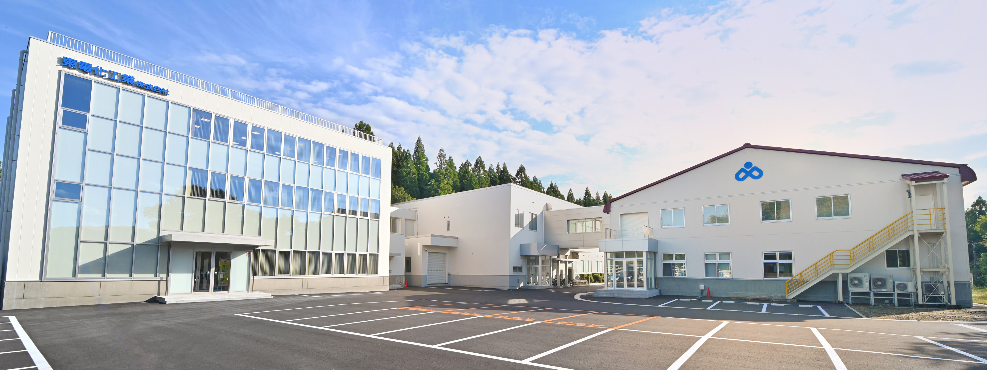
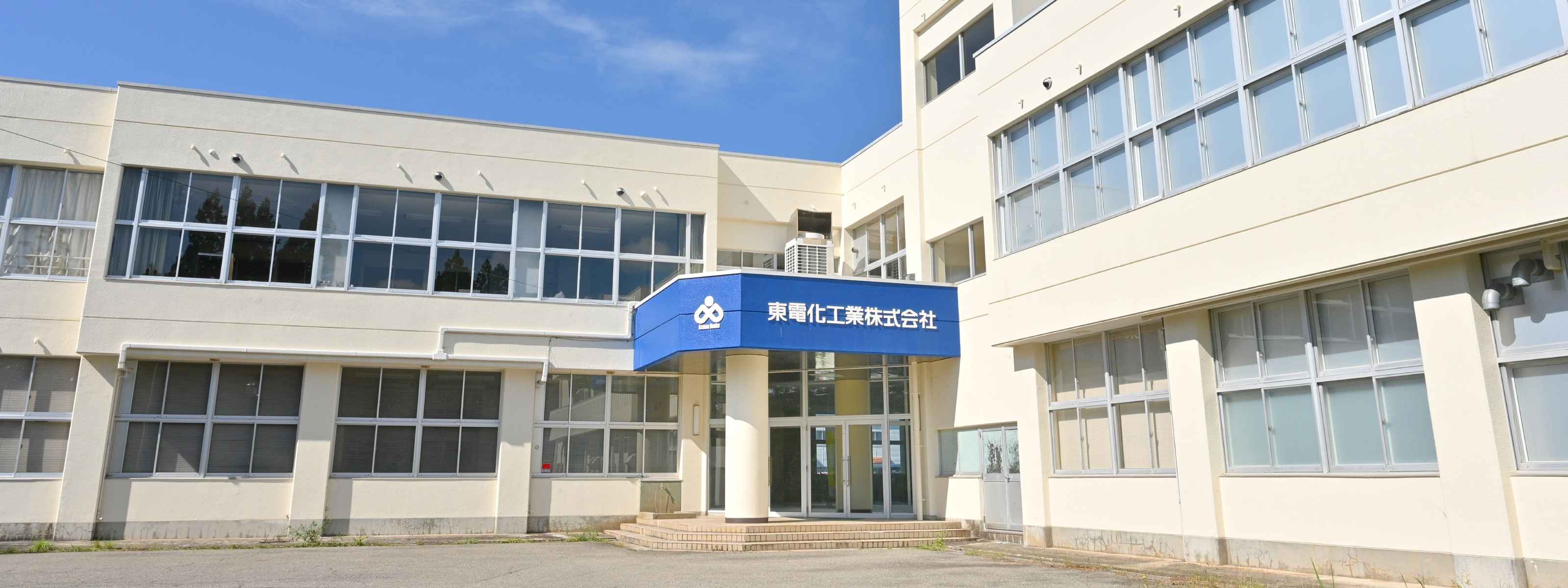
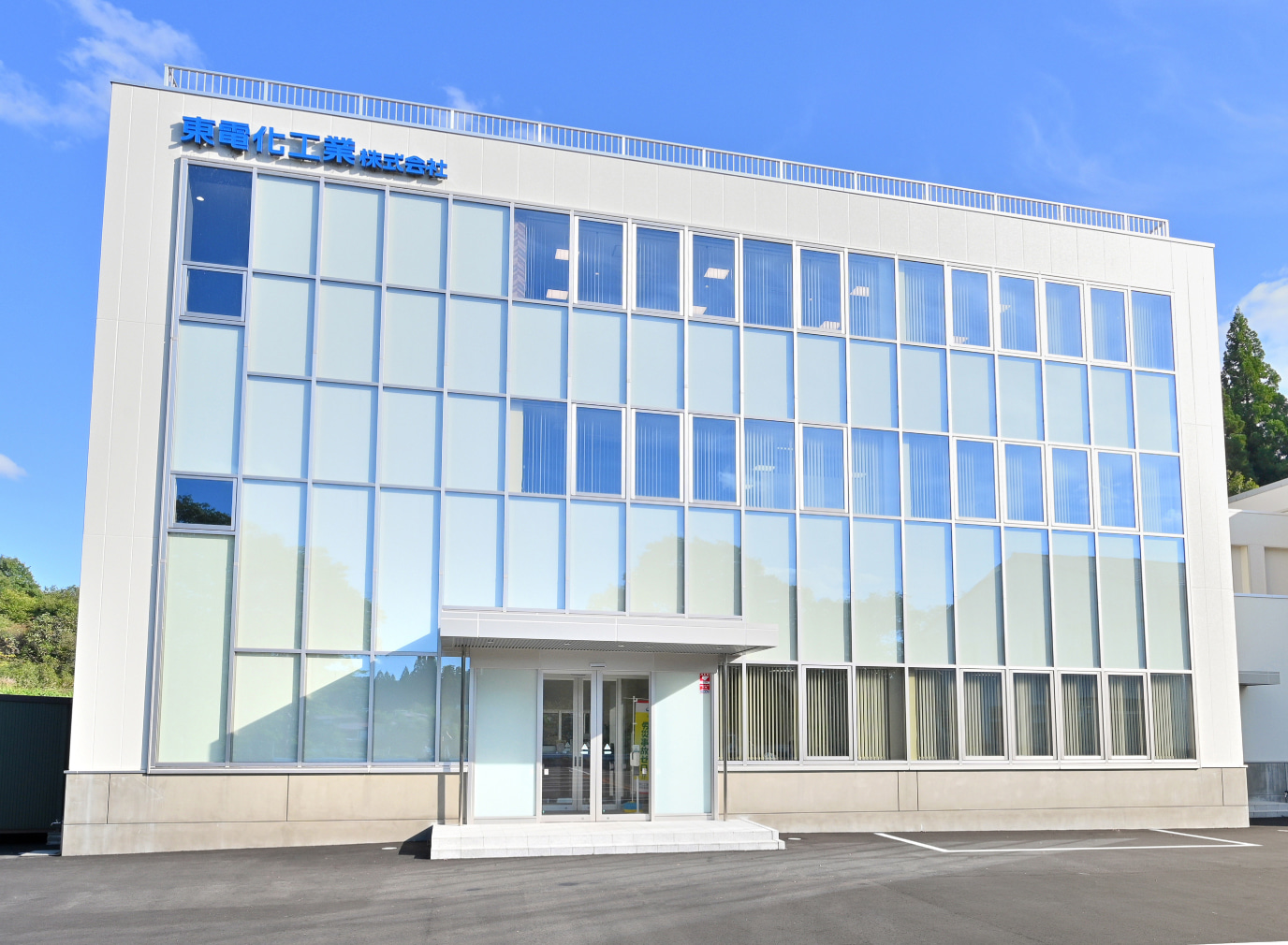
Our company started in 1946 in Higashimachi, Meguro-ku, Tokyo as a company engaged in anticorrosion and decorative plating of Ni/Cr plating. Then, in 1982, we were invited by Akita Prefecture to Kyowa-machi, Senboku-gun, Akita Prefecture (presently Kyowa, Daisen City), and began full-scale operations as the only plating company in the prefecture specializing in semiconductor electronic components.
Today, "plating" is an indispensable technology in our daily lives. Although this technology is used in automotive products and electronic components, we cannot actually see it because it is built into the products. However, we feel the value and joy of our technology when it is widely used by people all over the world. We will continue to run as a behind-the-scenes force.
>We have been able to continue our operations to this day thanks to the warm guidance of our customers.
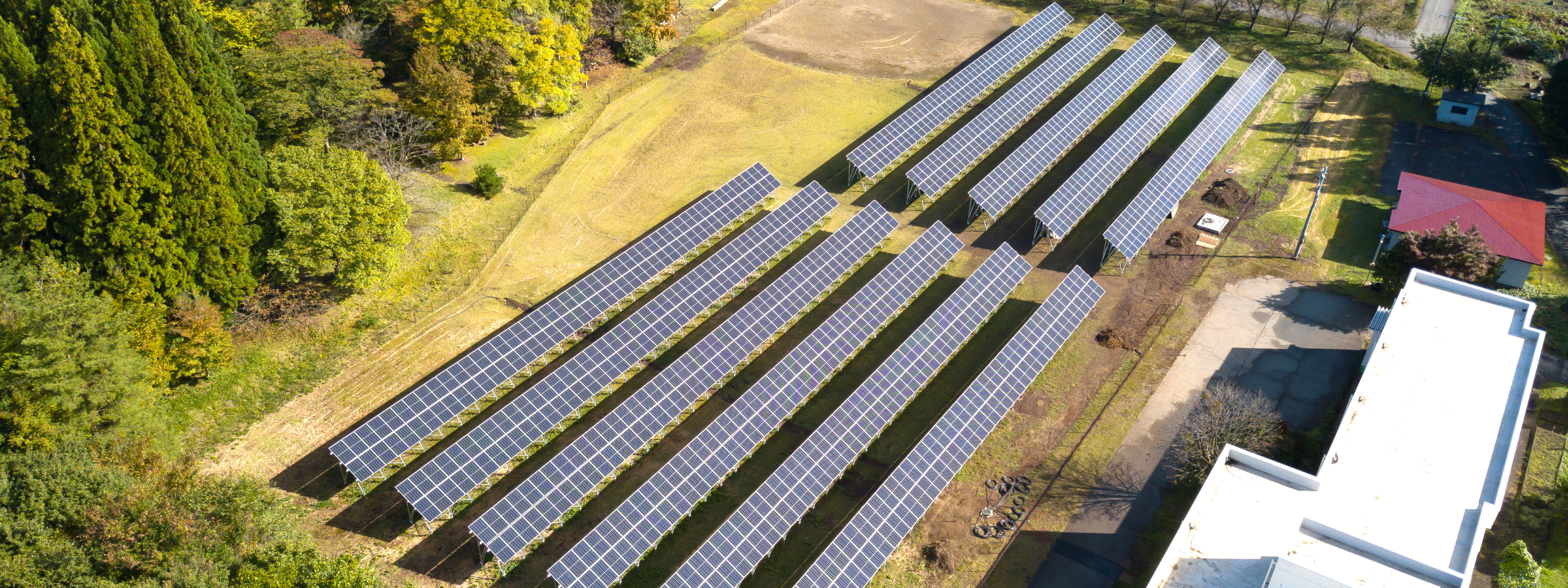
We will continue to strive to be a company that is friendly to the global environment and that satisfies our customers.
PRODUCT・SERVICE
Action, Cooperation, Challenge
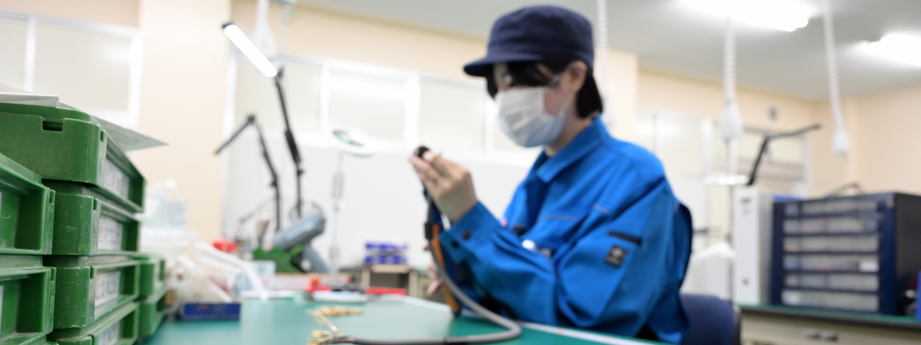
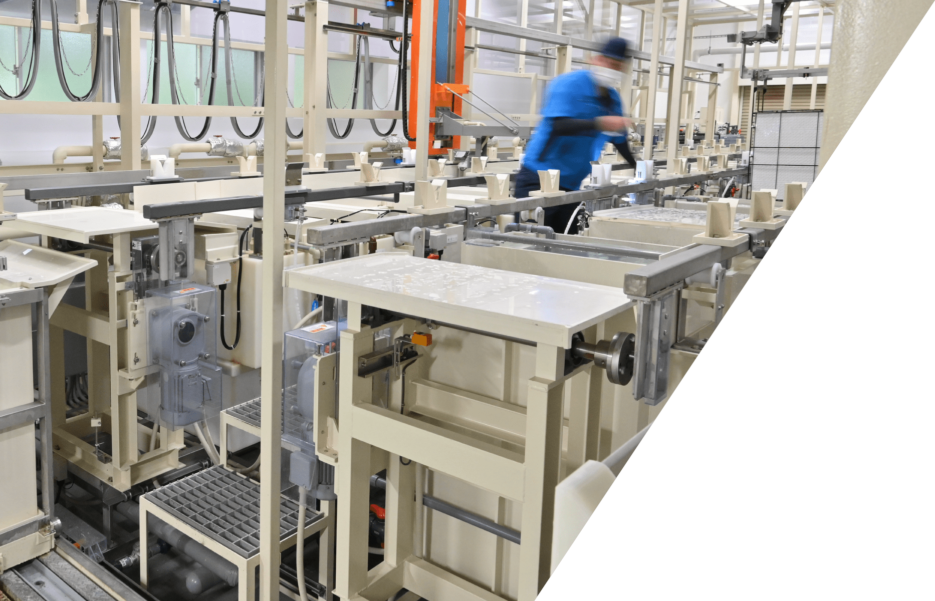
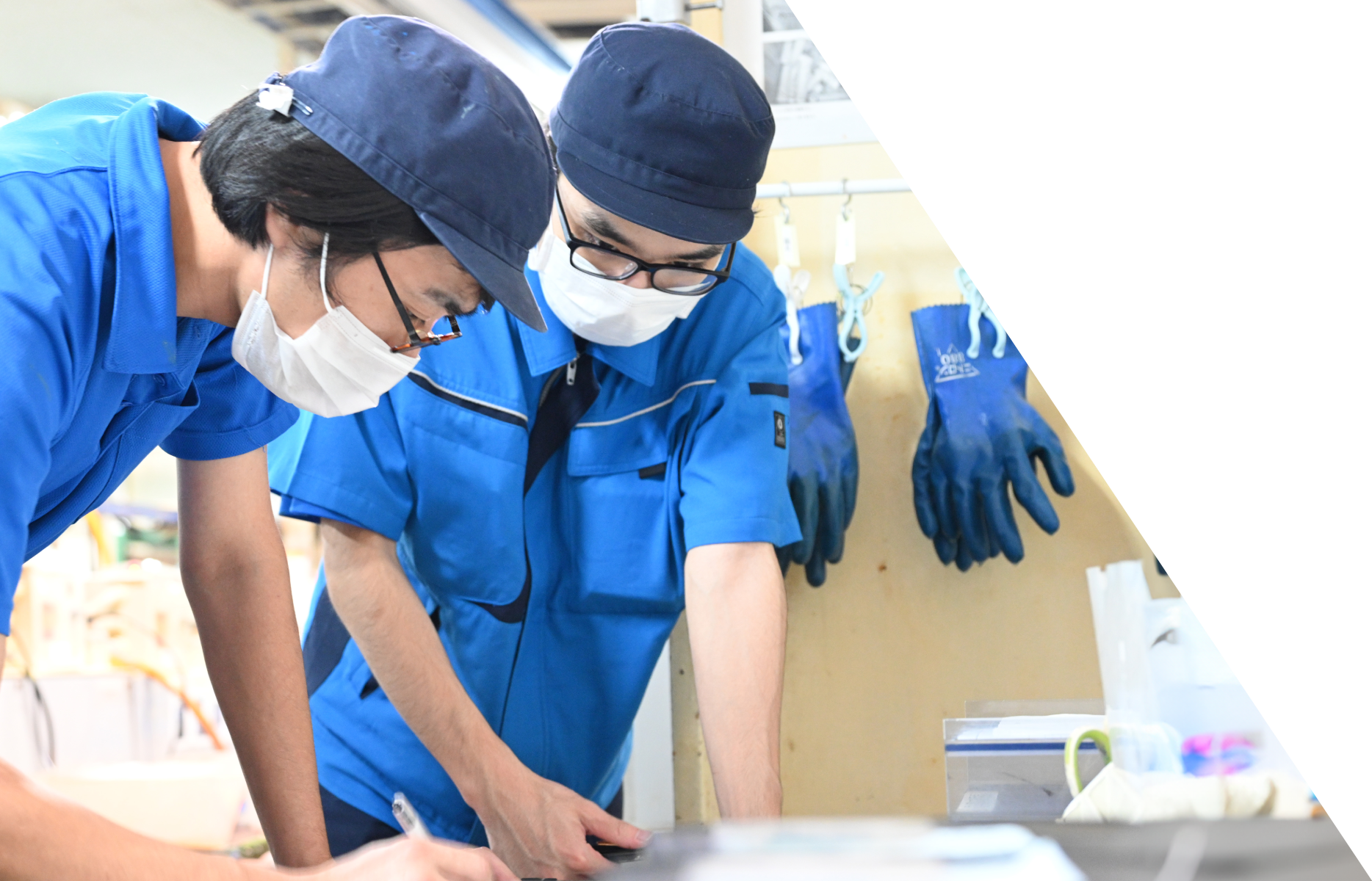
We carry out "monozukuri" (manufacturing) to meet the needs of our customers.
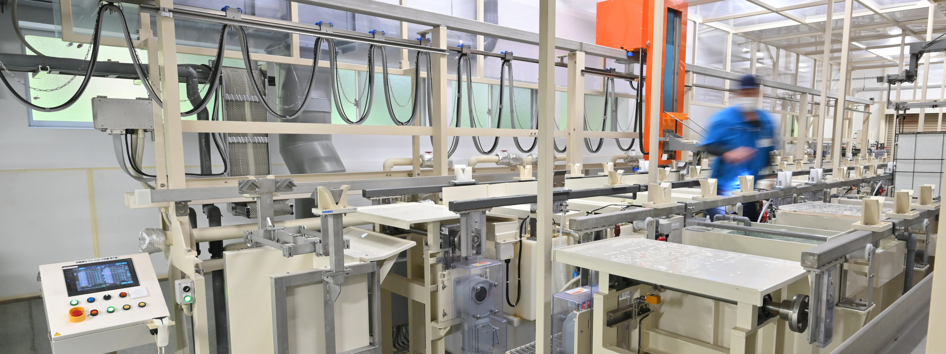
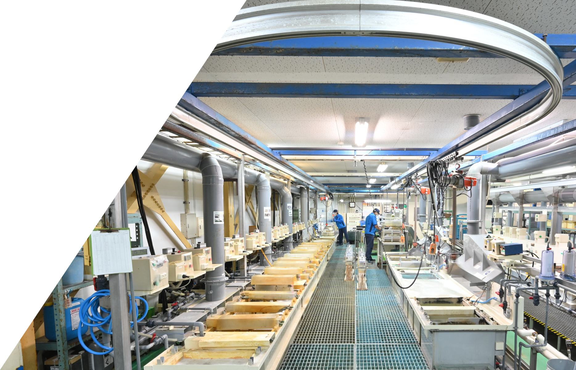
We have an automatic line capable of mass production and a manual line capable of small-lot, multi-variety production.
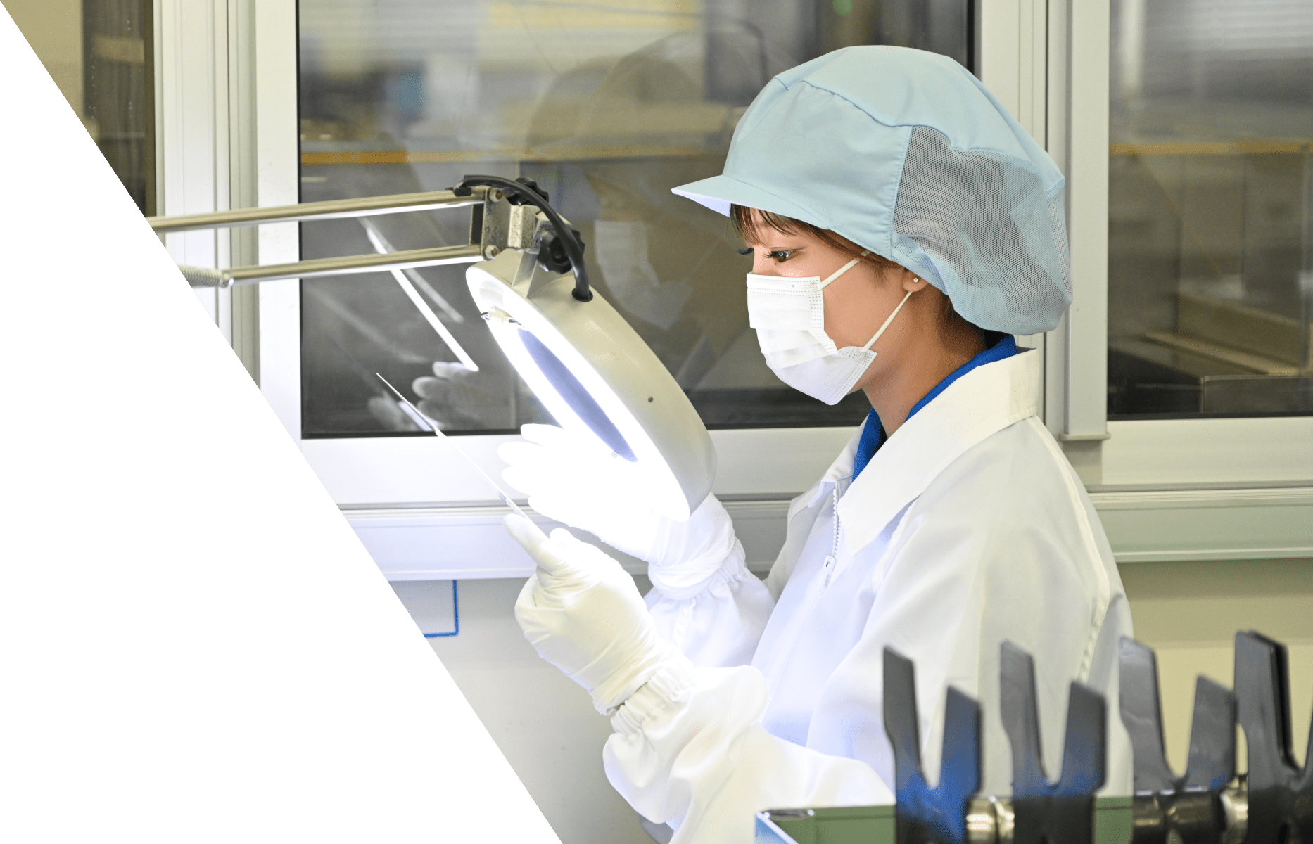
In order to study and propose processing methods that meet customer needs, we have established a laboratory to research and experiment with cutting-edge technologies on a daily basis.
In plating, we perform various types of plating on the wiring patterns of various substrates including LED substrates, so please contact us if you have any requests regarding plating specifications.
RECRUIT
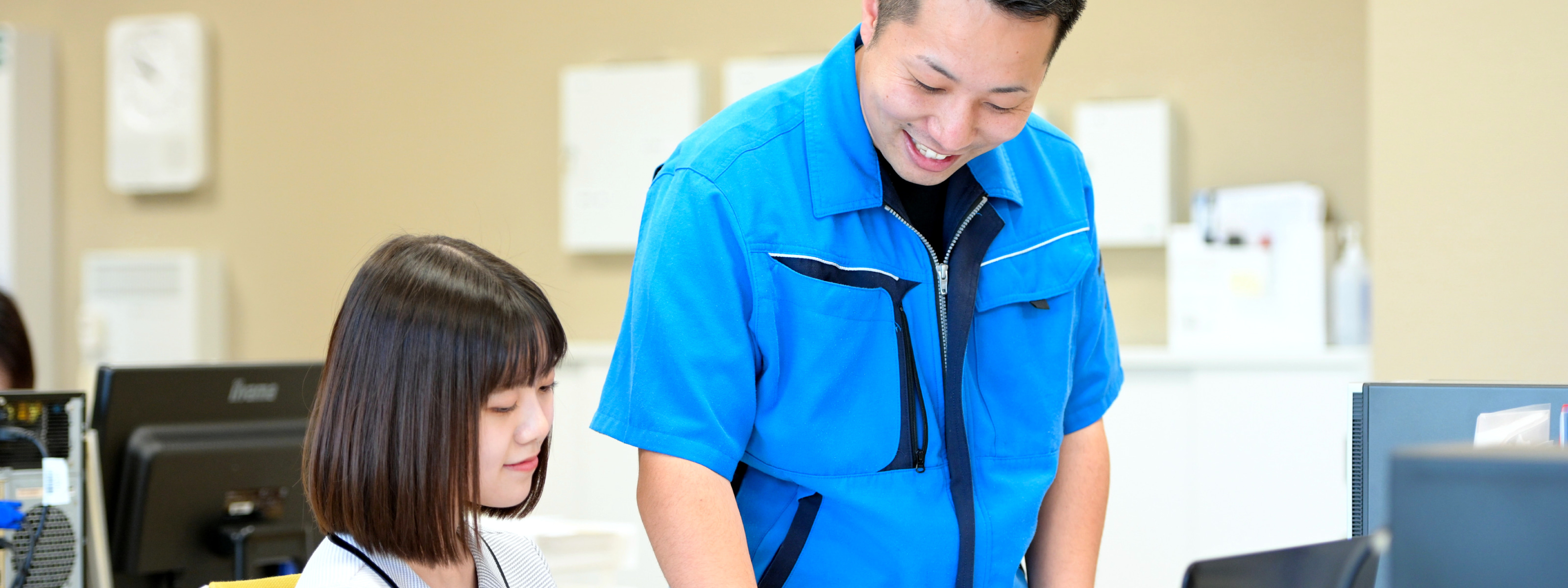
We are running full steam ahead to become the best plating shop in Japan!
The "No.1 plating shop in Japan" is not just about sales and profits. We aim to be the best plating shop in Japan, where people can think "I am happy to work for this company" and "I am glad to work for this company.
HAPPINESS
FOR EVERYONE
In order to realize "a company that creates happiness for everyone," we are working to change our organizational culture and are involved in SDG activities. We are also working on the AZUMA model to become a target organization.
ISO·CSR·BCP
We have acquired ISO 14001 and 9001 certification, and have created and are operating a business continuity plan and internal code of conduct to earn the trust of our customers, cooperating companies, and the local community.